


· Uses depth map intelligent noise reduction to solve 3D imaging distortion issues.
· Configurable measurement height range to suit a variety of application requirements.
· Uses dynamic adaptive reference plane technology for automatic substrate height correction.
· Multi-frequency algorithm increases robustness and reduces the impact of brightness changes on imaging.
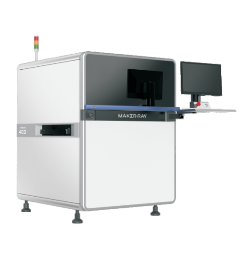
Online PCBA SMT 3D optical inspection equipment
Inspection of SMT components and solder defects
3D imaging, minimizing shadow issues
Core strengths:
· Uses depth map intelligent noise reduction to solve 3D imaging distortion issues.
· Configurable measurement height range to suit a variety of application requirements.
· Uses dynamic adaptive reference plane technology for automatic substrate height correction.
· Multi-frequency algorithm increases robustness and reduces the impact of brightness changes on imaging.
Detectable defect instances -Chip
Detectable defect instances -Cold Solder Joint
